
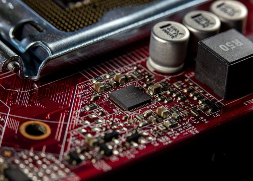
Electronic components on a computer motherboard, an illustrative archive photo from 2021. Photo: Sergei Starostin/Pexels, Pexels License. Cropped. Not identified as Panasonic products or an AI server.
Panasonic Industry said Friday it plans to invest approximately 92 billion yen to expand production of electronic materials and components used in AI servers, while building a research facility for the next generation of semiconductor-packaging materials.
The Panasonic Group operating company’s October 30 announcement spans Japan, China, Thailand and Indonesia. The investment targets the hardware supply chain behind AI computing: circuit-board materials that carry high-speed signals and capacitors that help maintain a stable power supply to graphics processors.
The plan is an expansion of components and materials production, not an announcement that Panasonic will build an AI processor fabrication plant.
67 billion yen for circuit-board materials
The largest part of the plan is approximately 67 billion yen for MEGTRON high-performance multilayer circuit-board materials at plants in Suzhou, China, and Ayutthaya, Thailand.
Panasonic Industry allocated approximately 30 billion yen to a new Phase II building in Suzhou, with operations scheduled to begin in August 2028. That follows a separate Phase I plant scheduled to begin mass production in December 2026.
Another approximately 37 billion yen will support a Phase II building in Ayutthaya, scheduled to start operations in April 2029. The site’s Phase I facility is scheduled to begin operations in November 2027.
The company said these materials support high-speed, high-capacity communication in AI servers and other equipment. It did not disclose a numerical increase in production capacity for the overall investment.
Capacitors for AI-server power circuits
Panasonic Industry also plans approximately 17 billion yen of investment across Uji, Japan, and Batam, Indonesia, to increase production of SP-Cap conductive polymer aluminum electrolytic capacitors.
Capacitors are electronic components that help stabilize power. Panasonic said SP-Cap devices are increasingly used in power circuits for graphics processing units and other AI-server components.
The Batam plan includes a new five-story manufacturing building with approximately 50,000 square meters of floor space. Construction is scheduled to begin in May 2027, with operations expected in April 2029.
New materials research in Japan
The remaining approximately 8 billion yen is planned for a new research and development building at Yokkaichi South Factory in Mie, Japan.
That facility will focus on materials used in semiconductor packaging, including package substrates and encapsulation materials. Packaging connects and protects chips, a growing design challenge as AI-server chips become larger and manufacturers use chiplet architectures.
Panasonic said the building will bring together materials development, prototyping and evaluation. It did not give an opening date for the research building in the announcement.
The company framed the expansion as a response to growing demand for generative AI infrastructure. The factories and research investment remain plans with future operating dates, rather than capacity already brought online.
Business Desk | TOKYO
© JBizNews.com. All rights reserved. Unauthorized reproduction or redistribution is strictly prohibited.